




Produkte
Laseranlagen
Laserschneidanlagen
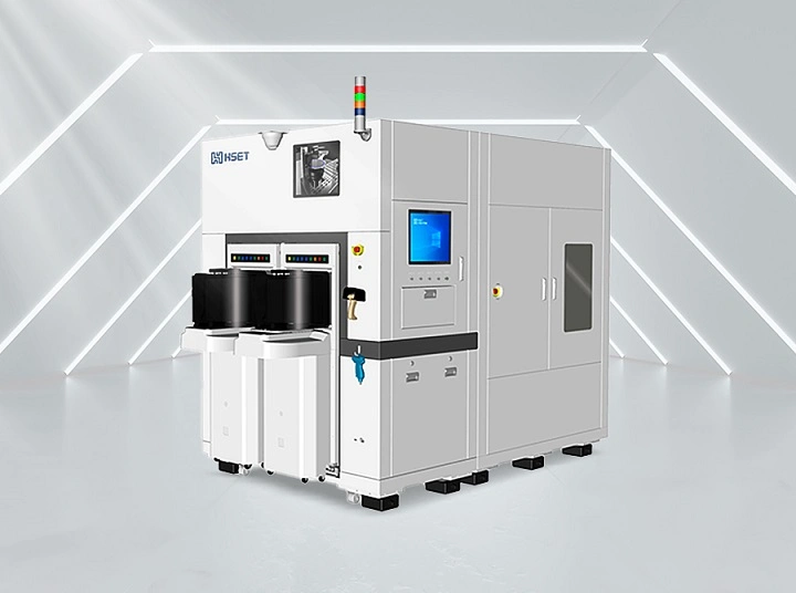
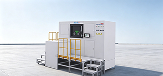
Lasertrennanlage für Wafer und Leiterplattenbaugruppen (PCBA)
CO₂-Laserschneidanlage
3D-Präzisions-Laserschneidanlage
Präzisions-Laserschneidanlage für spröde Werkstoffe
Sonstige Präzisions-Laserschneidanlagen
Laser-Abisolieranlage
Laserschneidanlage für mittlere und hohe Leistungen
Automatische Laserschneidanlage
Basiskomponenten
Kontakt
Anwendungsbereiche

Lösungen von Han’s Laser
Han’s Laser räumt F&E und technologischer Innovation seit jeher höchste Priorität ein. Heute verfügen wir über weltweit führende F&E-Kompetenzen in der Laserindustrie, gestützt auf mehr als 7.400 Patente. Aufbauend auf unseren Produktstärken erweitern wir kontinuierlich unsere durchgängigen Lösungen für ein breites Anwendungsspektrum, um die intelligente Fertigung in zahlreichen Branchen weltweit voranzutreiben.
Alle ansehen
Lithium-Ionen-Batterien für neue Energien
Photovoltaik (PV) und Solarenergie
Display- und Halbleiterindustrie
Leiterplattenindustrie
Elektronik- und Informationsindustrie
Maschinenbau und Metallwaren
Hausgeräte, Küche & Bad
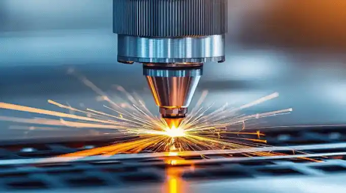
Blechbearbeitung
Verpackungsindustrie
Verkehrswesen
Textil- und Dekorationsindustrie
Automobilproduktion


Kontakt